AC 220 Volts Flashing Lamps Circuit

Especially designed for Christmas tree lamps, Replaces old thermally-activated switches


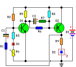
This circuit is intended as a reliable replacement to thermally-activated switches used for Christmas tree lamp-flashing. The device formed by Q1, Q2 and related resistors triggers the SCR. Timing is provided by R1, R2 & C1. To change flashing frequency do not modify R1 and R2 values: set C1 value from 100 to 2200µF instead.
Best performances are obtained with C1= 470 or 1000µF and R4= 12K or 10K. Due to low consumption of normal 10 or 20 lamp series-loops intended for Christmas trees (60mA @ 230V typical for a 20 lamp series-loop), very small and cheap SCR devices can be used, e.g. C106D1 (400V 3.2A) or TICP106D (400V 2A), this last and the suggested P0102D devices having TO92 cases.


Circuit diagram:

AC 220 Volts Flashing Lamps Circuit Diagram

Parts:
R1 = 100K
R2 = 1K
R3 = 470R
R4 = 12K
R5 = 1K
R6 = 470R
Q1 = BC327
Q2 = BC337
D1 = 1N4007
D2 = 1N4007
D3 = 1N4007
D4 = 1N4007
D5 = P0102D (SCR)
C1 = 1KµF-25V
PL1 = Male Mains plug
SK1 = Female Mains socket

Important Note:
For proper operation it is absolutely necessary to employ high Gate-sensitive SCRs.
If you are unable to find these devices you can use Triacs instead. In this case the circuit operates also with relatively powerful devices. A recommended Triac type is the ubiquitous TIC206M (600V 4A) but many others can work.
Please note that, in spite of the Triac, diode bridge D1-D4 is in any case necessary.

Warning! The device is connected to 230Vac mains, then some parts in the circuit board are subjected to lethal potential! Avoid touching the circuit when plugged and enclose it in a plastic box.

Led or Lamp Flasher Circuit

Ideal to operate 3 to 24V DC existing on-circuit lamps

This circuit was designed to provide that continuous light lamps already wired into a circuit, become flashing. Simply insert the circuit between existing lamp and negative supply. Especially suited for car or panel pilot lights, this device can drive lamps up to 10W.
Circuit diagram:

Led or Lamp Flasher Circuit Diagram

Parts:
R1 = 6.8K
R2 = 270K
R3 = 220K
D1 = 1N4002
C1 = 220uF-25V
C2 = 10uF-25V
Q1 = BC557
Q2 = BD139
B1 = Any type in the range 3-24V
B1 = Suited to the lamp adopted
LP1 = Filament Lamp 10W-3V to 24V
SW1 = On-Off Switch

Notes:
  • Break lamp to negative supply connection, and then insert the circuit between existing lamp connection and negative supply (respecting polarities!).
  • C1 value can be varied from 100 to 1000µF or higher, in order to change flashing frequency.
  • Although rather oversized, this circuit can also drive any LED, providing a suitable resistor is fitted in series with the light emitting device.
  • The resistor should lie in the 47R to 2K2 range, depending on supply voltage.

Mini Guitar/Bass Amplifier

Output power: 6W into 4 Ohm load, FET input stage - Passive Tone Control

Tiny, portable Guitar Amplifiers are useful for practice on the go and in bedroom/living room environment. Usually, they can be battery powered and feature a headphone output. This project is formed by an FET input circuitry, featuring a High/Low sensitivity switch, followed by a passive Tone Control circuit suitable to Guitar or Bass. After the Volume control, a 6W IC power amplifier follows, powered by a 12-14V dc external supply Adaptor or from batteries, and driving a 4 Ohm 10 or 13cm (4"/5") diameter car loudspeaker. Private listening by means of headphones is also possible.

Circuit diagram:
Mini Guitar-Bass Amplifier Circuit Diagram
Parts:

P1______________1M Linear Potentiometer
P2____________100K Log Potentiometer
R1_____________68K 1/4W Resistor
R2____________470K 1/4W Resistor
R3______________2K7 1/4W Resistor
R4______________8K2 1/4W Resistor
R5____________680R 1/4W Resistor
R6____________220K 1/4W Resistor
R7_____________39R 1/4W Resistor
R8______________2R2 1/4W Resistor
R9____________220R 1/4W Resistor
R10_____________1R 1/4W Resistor
R11___________100R 1/2W Resistor
R12_____________1K5 1/4W Resistor
C1____________100pF 63V Polystyrene or Ceramic Capacitor
C2,C5,C9,C14__100nF 63V Polyester Capacitors
C3____________100µF 25V Electrolytic Capacitor
C4_____________47µF 25V Electrolytic Capacitor
C6______________4n7 63V Polyester Capacitor
C7____________470pF 63V Polystyrene or Ceramic Capacitor
C8______________2µ2 25V Electrolytic Capacitor
C10___________470µF 25V Electrolytic Capacitor
C11____________22nF 63V Polyester Capacitor
C12__________2200µF 25V Electrolytic Capacitor
C13__________1000µF 25V Electrolytic Capacitor
D1______________3mm red LED
Q1____________BF245 or 2N3819 General-purpose N-Channel FET
IC1_________TDA2003 10W Car Radio Audio Amplifier IC
SW1,SW2________SPST toggle or slide Switches
J1____________6.3mm Mono Jack socket
J2____________6.3mm Stereo Jack socket (switched)
J3_____________Mini DC Power Socket
SPKR__________4 Ohm Car Loudspeaker 100 or 130mm diameter

Notes:
  • Connect the output Plug of a 12 - 14V dc 500mA Power Supply Adaptor to J3
  • Please note that if the voltage supply will exceed 18V dc the IC will shut down automatically
Technical data:

Output power (1KHz sinewave):
6W RMS into 4 Ohm at 14.4V supply
Sensitivity:
50mV RMS input for full output
Frequency response:
25Hz to 20kHz -3dB with the cursor of P1 in center position
Total harmonic distortion:
0.05 - 4.5W RMS: 0.15% 6W RMS: 10%

Tone Control Frequency Response:

10W Audio Amplifier With Bass-Boost

High Quality, very simple design, No preamplifier required

This design is based on the 18 Watt Audio Amplifier, and was developed mainly to satisfy the requests of correspondents unable to locate the TLE2141C chip. It uses the widespread NE5532 Dual IC but, obviously, its power output will be comprised in the 9.5 - 11.5W range, as the supply rails cannot exceed ±18V. As amplifiers of this kind are frequently used to drive small loudspeaker cabinets, the bass frequency range is rather sacrificed. Therefore a bass-boost control was inserted in the feedback loop of the amplifier, in order to overcome this problem without quality losses. The bass lift curve can reach a maximum of +16.4dB @ 50Hz. In any case, even when the bass control is rotated fully counterclockwise, the amplifier frequency response shows a gentle raising curve: +0.8dB @ 400Hz, +4.7dB @ 100Hz and +6dB @ 50Hz (referred to 1KHz).

Amplifier with Bass-Boost:
10W Bass Boost Amplifier Circuit Diagram
Parts:

P1_________________22K Log.Potentiometer (Dual-gang for stereo)
P2________________100K Log.Potentiometer (Dual-gang for stereo)
R1________________820R 1/4W Resistor
R2,R4,R8____________4K7 1/4W Resistors
R3________________500R 1/2W Trimmer Cermet
R5_________________82K 1/4W Resistor
R6,R7______________47K 1/4W Resistors
R9_________________10R 1/2W Resistor
R10__________________R22 4W Resistor (wirewound)
C1,C8_____________470nF 63V Polyester Capacitor
C2,C5_____________100µF 25V Electrolytic Capacitors
C3,C4_____________470µF 25V Electrolytic Capacitors
C6_________________47pF 63V Ceramic or Polystyrene Capacitor
C7_________________10nF 63V Polyester Capacitor
C9________________100nF 63V Polyester Capacitor
D1______________1N4148 75V 150mA Diode
IC1_____________NE5532 Low noise Dual Op-amp
Q1_______________BC547B 45V 100mA NPN Transistor
Q2_______________BC557B 45V 100mA PNP Transistor
Q3_______________TIP42A 60V 6A PNP Transistor
Q4_______________TIP41A 60V 6A NPN Transistor
J1__________________RCA audio input socket

Power Supply :
Power Supply Circuit Diagram
Power supply parts:

R11_________________1K5 1/4W Resistor
C10,C11__________4700µF 25V Electrolytic Capacitors
D2________________100V 4A Diode bridge
D3________________5mm. Red LED
T1________________220V Primary, 12 + 12V Secondary 24-30VA Mains transformer
PL1_______________Male Mains plug
SW1_______________SPST Mains switch

Notes:
  • Can be directly connected to CD players, tuners and tape recorders.
  • Schematic shows left channel only, but C3, C4, IC1 and the power supply are common to both channels.
  • Numbers in parentheses show IC1 right channel pin connections.
  • A log type for P2 will ensure a more linear regulation of bass-boost.
  • Do not exceed 18 + 18V supply.
  • Q3 and Q4 must be mounted on heatsink.
  • D1 must be in thermal contact with Q1.
  • Quiescent current (best measured with an Avo-meter in series with Q3 Emitter) is not critical.
  • Set the volume control to the minimum and R3 to its minimum resistance.
  • Power-on the circuit and adjust R3 to read a current drawing of about 20 to 25mA.
  • Wait about 15 minutes, watch if the current is varying and readjust if necessary.
  • A correct grounding is very important to eliminate hum and ground loops. Connect to the same point the ground sides of J1, P1, C2, C3 &C4. Connect C9 to the output ground.
  • Then connect separately the input and output grounds to the power supply ground.
Technical data:
Output power:
10 Watt RMS into 8 Ohm (1KHz sinewave)
Sensitivity:
115 to 180mV input for 10W output (depending on P2 control position)
Frequency response:
See Comments above
Total harmonic distortion @ 1KHz:
0.1W 0.009% 1W 0.004% 10W 0.005%
Total harmonic distortion @ 100Hz:
0.1W 0.009% 1W 0.007% 10W 0.012%
Total harmonic distortion @ 10KHz:
0.1W 0.056% 1W 0.01% 10W 0.018%
Total harmonic distortion @ 100Hz and full boost:
1W 0.015% 10W 0.03%
Max. bass-boost referred to 1KHz:
400Hz = +5dB; 200Hz = +7.3dB; 100Hz = +12dB; 50Hz = +16.4dB; 30Hz = +13.3dB
Unconditionally stable on capacitive loads

DCF77 Preamplifier

A popular project among microcontroller aficionados is to build a radio-controlled clock. Tiny receiver boards are available, with a pre-adjusted ferrite antenna, that receive and demodulate the DCF77 time signal broadcast from Mainf lingen in Germany. DCF77 has a range of about 1,000 miles. All the microcontroller need do is decode the signal and output the results on a display. The reception quality achieved by these ready-made boards tends to be proportional to their price.

In areas of marginal reception a higher quality receiver is needed, and a small selective preamplifier stage will usually improve the situation further. The original ferrite antenna is desoldered from the receiver module and connected to the input of the preamplifier. This input consists of a source follower (T1) which has very little damping effect on the resonant circuit. A bipolar transistor (T2) provides a gain of around 5 dB. The output signal is coupled to the antenna input of the DCF77 module via a transformer.

Circuit diagram:
DCF77 Preamplifier Circuit Diagram
The secondary of the transformer, in conjunction with capacitors C4 and C5, forms a resonant circuit which must be adjusted so that it is centered on the carrier frequency. An oscilloscope is needed for this adjustment, and a signal generator, set to generate a 77.5 kHz sine wave, is also very useful. This signal is fed, at an amplitude of a few milli-volts, into the antenna input. With the oscilloscope connected across C4 and C5 to monitor the signal on the output resonant circuit, trimmer C5 is adjusted until maximum amplitude is observed.

It is essential that the transformer used is suitable for constructing a resonant circuit at the carrier frequency. Our proto-type used a FT50-77 core from Amidon on which we made two 57-turn windings. It is also possible to trim the resonant frequency of the circuit by using a transformer whose core can be adjusted in and out. In this case, of course, the trimmer capacitor can be dispensed with.
Rainer Reusch
Elektor Electronics 2008

Blinker Indicator

This circuit represents a somewhat unusual blinker indicator for use in a car or model. The running-light display progresses toward the left or the right depending on which directional signal is activated. That’s pretty cool if you’re fond of light-show effects. The circuit consists of two counters (IC2 and IC3), which are reset to zero via C4 or C7 respectively whenever a blinker lamp (La) illuminates. The running-light display thus runs through once and then stops, since the highest counter output is connected to the Enable input.

Circuit diagram:
Blinker Indicator Circuit Diagram

When the lamp goes out, a new reset pulse is issued to the relevant counter by NAND gate IC1.A or IC1.B respectively, and the counter counts all the way up again. The progression rate of the display can be adjusted to the right speed using P1. Only one LED is on at a time (except for the hazard blinker). This allows the brightness to be easily adjusted using R12. Incidentally, the circuit can also be modified by replacing the normal diodes with LEDs, with all of the cathodes connected to ground via R12.
Author: Ludwig Libertin - Copyright: Elektor July-August 2004

Discrete PWM Generator Circuit

PWM waveforms are commonly used to control the speed of DC motors. The mark/space ratio of the digital wave-form can be defined either by using an adjustable analogue voltage level (in the case of a NE555 based PWM generator) or digitally using binary values. Digitally derived PWM waveforms are most often produced by the timer/counter modules in microcontrollers but if you do not want to include a microcontroller in your circuit it’s also quite simple to generate the signals using discrete logic components.

Circuit diagram:

Discrete PWM Generator Circuit Diagram

An extension of the circuit shown can produce two PWM wave-forms from an 8-bit digital input word. Each signal has 15 values. The 8-bit word can be produced for example from an expansion board fitted in a PC or from an 8-bit port of a processor which does not have built-in PWM capability or from a laptop’s printer port. The mark/space ratio is only programmable up to 15/16 rather than 16/16; a binary input of 0000 produces a continuous low on both outputs turning both motors off.

Similar circuits often employ a dedicated ‘enable’ input to turn the motors off but it is not necessary in this design. The diagram shows the circuitry required to produce just one waveform. For the full two channel circuit it is necessary to use an additional 74HC193. The clock signal produced by the HCF4060 generator can be used to drive both channels and the free flip flop in the 74HC74 package can be used for the second channel (the corresponding pin numbers are shown in brackets). Altogether the entire two channel circuit can be built using just four ICs.

Source: extremecircuits.net

Mains Failure Alarm

This circuit was designed to produce an audible alarm when the mains power is interrupted. Such an alarm is essential for anyone whose livelihood depends on keeping perishable foodstuffs in cold storage. The circuit is powered by a 12-V mains adapter. LED D5 will light when the mains voltage is present. When the mains voltage disappears, so does the +12 V supply voltage, leaving the voltage regulator IC1 and relay driver T1-T2 without power. The relay driver, by the way, is an energy-saving type, reducing the coil current to about 50% after a few seconds. Its operation and circuit dimensioning are discussed in the article ‘Relay Coil Energy Saver’. The value of the capacitor at the output of voltage regulator IC1 clearly points to a different use than the usual noise suppression.

Circuit diagram:
Mains Failure Alarm Circuit Diagram

When the mains power disappears, Re1 is de-energized and the 0.22 F Gold-cap used in position C4 provides supply current to IC2. When the mains voltage is present, C4 is charged up to about 5.5 volts with IC1 acting as a 100-mA current limit and D10 preventing current flowing back into the regulator output when the mains voltage is gone. According to the Goldcap manufacturer, current limiting is not necessary during charging but it is included here for the security’s sake. The CMOS 555 is configured in astable multivibrator mode here to save power, and so enable the audible alarm to sound as long as possible. Resistors R5 and R6 define a short ‘on’ time of just 10 ms. That is, however, sufficient to get a loud warning from the active buzzer. In case the pulses are too short, increase the value of R5 (at the expense of a higher average current drawn from the Goldcap).
Author: Myo Min - Copyright: Elektor July-August 2004

1W LED Driver

This circuit is designed to drive the 1W LEDs that are now commonly available. Their non-linear voltage to current relationship and variation in forward voltage with temperature necessitates the use of a 350mA, constant-current power source as provided by this supply. In many respects, the circuit operates like a conventional step-down (buck) switching regulator. Transistor Q1 is the switching element, while inductor L1, diode D1 and the 100mF capacitor at the output form the energy transfer and storage elements. The pass transistor (Q1) is switch-ed by Q2, which together with the components in its base circuit, forms a simple oscillator. A 1nF capacitor provides the positive feedback necessary for oscillation. The output current is sensed by transistor Q3 and the two parallelled resistors in its base-emitter circuit.

Circuit diagram:

1W LED Driver Circuit Diagram

When the current reaches about 350mA, the voltage drop across the resistors exceeds the base-emitter forward voltage of transistor Q3 (about 0.6V), switching it on. Q3’s collector then pulls Q2’s base towards ground, switching it off, which in turn switches off the main pass transistor (Q1). The time constant of the 15kW resistor and 4.7nF capacitor connected to Q2’s base adds hysteresis to the loop, thus ensuring regulation of the set output current. The inductor was made from a small toroid salvaged from an old computer power supply and rewound with 75 turns of 0.25mm enamelled copper wire, giving an inductance of about 620mH. The output current level should be trimmed before connecting your 1W LED. To do this, wire a 10W 5W resistor across the output as a load and adjust the value of one or both of the resistors in the base-emitter circuit of Q3 to get 3.5V (maximum) across the load resistor.
Author: Nick Baroni - Copyright: Silicon Chip

LED Light Pen

Physicians and repair engineers often use small light pens for visual examination Spurposes. Rugged and expensive as these pens may be, their weak point is the bulb, which is a ‘serviceable’ part. In practice, that nearly always equates to ‘expensive’ and / or ‘impossible to find’ when you need one. LEDs have a much longer life than bulbs and the latest ultra bright white ones also offer higher energy-to-light conversion efficiency. On the down side, LEDs require a small electronic helper circuit called ‘constant-current source’ to get the most out of them. Here, T1 and R1 switch on the LED. R2 acts as a current sensor with T2 shunting off (most of) T1’s base bias current when the voltage developed across R2 exceeds about 0.65 V.

Circuit diagram:
LED Light Pen Circuit Diagram

The constant current through the white LED is calculated from R2 = 0.65 / I LED With some skill the complete circuit can be built such that its size is equal to an AA battery. The four button cells take the place of the other AA battery that used to be inside the light pen.
Author: Myo Min - Copyright: Elektor July-August 2004

UV Torch Light

UV (ultra-violet) LEDs can produce eye-catching effects when their light is allowed to interfere with certain colours, particularly with reflected light under near-dark conditions. Also try shining some UV light on a diamond… Most UV LEDs require about 3.6 V (the ‘blue’ diode voltage) to light. Here, a MAX761 step-up switching IC is used to provide constant current to bias the UV diode. The IC employs PWM in high-current mode and automatically changes to PFM mode in low or medium power mode to save (battery) power. To allow it to be used with two AA cells, the MAX761 is configured in bootstrapped mode with voltage-adjustable feedback. Up to four cells may be used to power the circuit but they may add more weight than you would like for a torchlight. To prolong the switch life, R1 is connected to the IC’s SHDN (shutdown) pin. Less than 50 nA will be measured in shutdown mode.

Circuit diagram:

UV Torch Light Circuit Diagram

Electrolytic capacitor C1 is used to decouple the circuit supply voltage. Without it, ripple and noise may cause instability. The one inductor in the circuit, L1, may have any value between about 10 and 50 µH. It stores current in its magnetic field while the MOSFET inside the MAX761 is switched. A toroid inductor is preferred in this position as it will guarantee low stray radiation. D1 has to be a relatively fast diode so don’t be tempted to use an 1N400x because it has a too slow recovery time. The circuit efficiency was measured at about 70%. R2, the resistor on the feedback pin of the MAX761 effectively determines the amount of constant current, I, sent through the UV LEDs, as follows: R2 = 1.5 / I where I will be between 2 mA and 35 mA. Zener diode D4 clamps the output voltage when the load is disconnected, which may happen when one of the UV LEDs breaks down. Without a load, the MAX761 will switch L1 right up to the boost voltage and so destroy itself.
Author: Myo Min - Copyright: Elektor Electronics 2004

4-Bit Analogue to Digital Converter

The operation of the converter is based on the weighted adding and transferring of the analogue input levels and the digital output levels. It consists of comparators and resistors. In theory, the number of bits is unlimited, but each bit needs a comparator and several coupling resistors. The diagram shows a 4-bit version. The value of the resistors must meet the following criteria:
  • R1:R2 = 1:2;
  • R3:R4:R5 = 1:2:4;
  • R6:R7:R8:R9 = 1:2:4:8.
The linearity of the converter depends on the degree of precision of the value of the resistors with respect to the resolution of the converter, and on the accuracy of the threshold voltage of the comparators. This threshold level must be equal, or nearly so, to half the supply voltage. Moreover, the comparators must have as low an output resistance as possible and as high an input resistance with respect to the load resistors as feasible. Any deviation from these requirements affects the linearity of the converter adversely.

Circuit diagram:

4-Bit Analogue to Digital Converter Circuit Diagram

If the value of the resistors is not too low, the use of inverters with an FET (field-effect transistor) input leads to a near-ideal situation. In the present converter, complementary metal-oxide semiconductor (CMOS) inverters are used, which, in spite of their low gain, give a reasonably good performance. If standard comparators are used, take into account the output voltage range and make sure that the potential at their non-inverting inputs is set to half the supply voltage. If high accuracy is a must, comparators Type TLC3074 or similar should be used.

This type has a totem-pole output. The non-inverting inputs should be interlinked and connected to the tap of a a divider consisting of two 10 kΩ resistors across the supply lines. It is essential that the converter is driven by a low-resistance source. If necessary, this can be arranged via a suitable op amp input buffer. The converter draws a current not exceeding 5 mA.

12V Flourescent Lamp Inverter

Fluorescent tubes use far less energy than incandescent lamps and fluorescent tubes last a great deal longer as well. Other advantages are diffuse, glare-free lighting and low heat output. For these reasons, fluorescent lighting is the natural choice in commercial and retail buildings, workshops and factories. For battery-powered lighting, fluorescent lights are also the first choice because of their high efficiency. The main drawback with running fluorescent lights from battery power is that an inverter is required to drive the tubes.

Circuit diagram:
12V Fluorescent Lamp Inverter Circuit Diagram
Fig.1: two switch-mode circuits are involved here: the DC-DC inverter involving IC1, Q1 & Q2 and the fluoro tube driver which converts high voltage DC to AC via IC3 and Q3 & Q4 in a totem-pole circuit.

Inverter efficiency then becomes the major issue. There are many commercial 12V-operated fluorescent lamps available which use 15W and 20W tubes. However, it is rare to see one which drives them to full brilliance. For example, a typical commercial dual 20W fluorescent lamp operating from 12V draws 980mA or 11.8W. Ignoring losses in the fluorescent tube driver itself, it means that each tube is only supplied with 5.9W of power which is considerably less than their 20W rating. So while the lamps do use 20W tubes, the light output is well below par.

Warning:
This circuit generates in excess of 300V DC which could be lethal. Construction should only be attempted by those experimenced with mains-level voltages and safety procedures

Source: extremecircuits.net

Irregular Flasher

Two multivibrators with different frequencies can be built using the NAND gates of a 4011 IC. If the output of IC1.B is positive with respect to IC1.C, LED D1 is on. As the levels of IC1.A and IC1.D are exactly opposite, D2 is always on when D1 is off, and the other way around. The two oscillators have different frequencies, which are determined by the values of R2/C2 and R5/C5 respectively according to the formula f0 = 1 ÷ (1.4 RC) With the given component values, the frequencies are 2.2 Hz and 7.2 Hz. Low-current LEDs should be used, since the CMOS IC cannot sink or source sufficient current for ‘normal’ LEDs.

Circuit diagram:
Irregular Flasher Circuit Diagram

The values of series resistors R3 and R6 are suitable for a supply voltage of 12 V, in which case the current consumption of the circuit is around 5 mA. However, in principle the 4011 can be operated over a supply voltage range of 5–15 V. Higher currents can be provided by the HC family (supply voltage 3–6 V) or the HCT family (5 V). Incidentally, the part number of the quad gate IC in the HC family is HC7400.
Author: Ludwig Libertin - Copyright: Elektor July-August 2004

Two-Led Pilot Light

220vAC mains operated, Very simple circuitry

This circuit is designed on request and can be useful to those whishing to have, say, a red LED illuminated when an appliance is on and a green LED illuminated when the same appliance is off. Any mains operated appliance can be monitored by this circuit provided a suitable mains switch, capable of withstanding the full load current, is used for SW1.When SW1 is closed, the load and D4 are energized, Q1 is saturated and shorts D3, thus preventing its illumination.
Circuit Diagram:


Parts:

R1 = 27K-1W
R2 = 27K-1W
R3 = 6.8K
D1 = 1N4007
D2 = 1N4007
D3 = Green
D4 = Red Led
Q1 = BC337
SW1 = SPST Mains Switch

Notes:
  • Change R1 and R2 to 15K 1W for 115Vac mains operation.
  • SW1 must be capable of withstanding the appliance's full load current and voltage.
Source : www.redcircuits.com

Model Theatre Lighting Dimmer

This circuit is the basis for the dimmers in a model theatre lighting system which uses touch globes as the light source. The circuit is based around a 555 timer, driving a Triac. All dimmers share the one power supply and zero-crossing detector. As it will only work if there is a common AC/DC return path, it has a simple DC supply circuit consisting of one 1N4004 diode and one 4700µF capacitor. Transistors Q1 to Q3 comprise a zero-crossing detector whose output is inverted into a negative-going pulse by Q4. This pulse is fed to the trigger input (pin 2) of the 555 IC which then starts its timing period at the beginning of each mains half cycle.

Circuit diagram:
Model Theatre Lighting Dimmer Circuit Diagram

The length of this period is set by capacitor C2 and the combination of resistors R6 with pots VR1 and VR2. The output of IC1 at pin 3 is then fed to transistor Q5 which inverts this signal to trigger the Triac via a 100# resistor. When the timing period is short, the Triac is turned on early in half cycle and lights are bright. Conversely, when the timing period is longer, the lights are dim or turned off. The main dimmer control is potentiometer VR1. Trimpot VR1 is used to set the range of VR1. With VR1 set fully clockwise (ie, maximum resistance) trimpot VR2 is adjusted until the lights are just turned off. The lights should then be able to be faded over the full range by the control potentiometer.
Author: Barry Freeman - Copyright: Silicon Chip Electronics

Tracking Down Scratchy Pots

One of the most common faults in audio equipment is noisy pots - potentiometers that introduce scratching or crackling noises into the signal as they are adjusted. The problem is that sometimes a perfectly good pot will sound scratchy or crackly because of an intermittent connection or because DC is getting into it through a faulty capacitor or an out of balance direct-coupled stage. So how can you determine whether a pot really is scratchy before going to the trouble of finding and fitting a physically compatible replacement?


This solution is simple and involves a test setup which can be done with the pot still in circuit (but with the power off). Using clip leads or temporarily soldered wires connected directly to the pot's terminals, connect the pot as a volume control between a signal generator and a signal tracer (or audio amplifier), as shown. Then adjust the pot up and down. If the signal tracer gives scratchy noises on top of the tone from the signal generator, then the pot is faulty.
Author: Andrew Partridge - Copyright: Silicon Chip Electronics

Hearing Aid

Portable and easy to built, Uses 1x3v battery

Commercially available hearing aids are quite costly. Here is an inexpensive hearing aid circuit that uses just four transistors and a few passive components.
Circuit Diagram:

Hearing Aid Circuit Diagram

Parts:
R1 = 2.2K
R2 = 680K
R3 = 3.3k
R4 = 220K
R5 = 1.5K
R6 = 220R
R7 = 100K
R8 = 680K
C1 = 104pF
C2 = 104pF
C3 = 1uF/10V
C4 = 100uF/10V
C5 = 100uF/10V
Q1 = BC549
Q2 = BC548
Q3 = BC548
Q4 = BC558
J1 = Headphone jack
B1 = 2x1.5V Cells
SW1 = On/Off-Switch

Circuit Operation:
On moving power switch SW1 to ‘on’ position, the condenser microphone detects the sound signal, which is amplified by Q1 and Q2. Now the amplified signal passes through coupling capacitor C3 to the base of Q3.
The signal is further amplified by Q4 to drive a low impedance earphone. Capacitors C4 and C5 are the power supply decoupling capacitors. The circuit can be easily assembled on a small, general-purpose PCB or a Vero board.
It operates off a 3V DC supply. For this, you may use two small 1.5V cells. Keep switch S to ‘off’ state when the circuit is not in use. To increase the sensitivity of the condenser microphone, house it inside a small tube.

Source : www.electronicsforu.com

Clap Sensitive On-Off Relay

3V Battery operated, Small portable unit

This circuit was intended to activate a relay by means of a hand clap. Further claps will turn-off the relay. An interesting and unusual feature of this project is the 3V battery operation. The circuit's sensitivity was deliberately reduced, in order to avoid unpredictable operation. Therefore, a loud hand clap will be required to allow unfailing on-off switching. Q1 acts as an audio amplifier. IC1 timer, wired as a monostable, provides a clean output signal and a reasonable time delay in order to allow proper switching of the following bistable circuit. A discrete-components circuit formed by Q2, Q3 and related parts was used for this purpose, in order to drive the Relay directly and to allow 3V supply operation.
Circuit Diagram:

Clap Sensitive on-off Relay Circuit Diagram

Parts:
R1 = 12K
R2 = 1M
R3 = 6.8K
R4 = 220K
R5 = 2.2M
R7 = 100K
R8 = 22K
R9 = 6.8K
R10 = 100K
Q1 = BC550C
Q2 = BC328
Q3 = BC328
C1 = 220nF-63V
C2 = 22nF-63V
C3 = 220nF-63V
C4 = 22nF-63V
C5 = 22nF-63V
C6 = 47uF-25V
D1 = 1N4148
D2 = 1N4148
B1 = 3V Battery
IC1 = 7555 CMos IC
RL1 = DIL Reed-Relay SPDT
SW1 = SPST Switch
MIC1 = Electret Mic

Notes:
A small DIL 5V reed-relay was used in spite of the 3V supply. Several devices of this type were tested and it was found that all of them were able to switch-on with a coil voltage value comprised in the 1.9 - 2.1V range. Coil resistance values varied from 140 to 250 Ohm. Stand-by current consumption of the circuit is less than 1mA. When the Relay is energized, current drain rises to about 20mA.

Dimmer With A MOSFET

This circuit shows that dimmers intended for use at mains voltage do not always have to contain a triac. Here, a MOSFET (BUZ41A, 500 V/4.5A) in a diode bridge is used to control the voltage across an incandescent bulb with pulse-width modulation (PWM). A useful PWM controller can be found elsewhere in this issue. The power supply voltage for driving the gate is supplied by the voltage across the MOSFET. D6, R5 and C2 form a rectifier. R5 limits the current pulses through D6 to about 1.5 A (as a consequence it is no longer a pure peak rectifier). The voltage across C2 is regulated to a maximum value of 10 V by R3, R4, C1 and D1. An optocoupler and resistor (R2) are used for driving the gate.

R1 is intended as protection for the LED in the optocoupler. R1 also functions as a normal current limiting device so that a ‘hard’ voltage can be applied safely. The optocoupler is anold acquaintance, the CNY65, which provides class-II isolation. This ensures the safety of the regulator. The transistor in the optocoupler is connected to the positive power supply so that T1 can be brought into conduction as quickly as possible. In order to reduce switching spikes as a consequence of parasitic inductance, the value of R2 has been selected to be not too low: 22 kΩ is a compromise between inductive voltages and switching loss when going into and out of conduction.

Circuit diagram:
Dimmer With A MOSFET Circuit Diagram

An additional effect is that T1 will conduct a little longer than what may be expected from the PWM signal only. When the voltage across T1 reduces, the voltage across D1 remains equal to 10 V up to a duty cycle of 88 %. A higher duty cycle results in a lower voltage. At 94 % the voltage of 4.8 V proved to be just enough to cause T1 to conduct sufficiently. This value may be considered the maximum duty cycle. At this value the transistor is just about 100 % in conduction. At 230 V mains voltage, the voltage across the lamp is only 2.5 V lower, measured with a 100-W lamp. Just to be clear, note that this circuit cannot be used to control inductive loads. T1 is switched asynchronously with the mains frequency and this can cause DC current to flow.

Electronic lamps, such as the PL types, cannot be dimmed with this circuit either. These lamps use a rectifier and internally they actually operate off DC.A few remarks about the size of R3 and R4. This is a compromise between the lowest possible current consumption (when the lamp is off) and the highest possible duty cycle that is allowed. When the duty cycle is zero, the voltage across the resistors is at maximum, around 128 V with a mains voltage of 230 V. Because (depending on the actual resistor) the voltage rating of the resistor may be less than 300 V, two resistors are connected in series. The power that each resistor dissipates amounts to a maximum of 0.5 W. With an eye on the life expectancy, it would be wise to use two 1-W rated resistors here.
Author: Ton Giesberts - Copyright: Elektor Electronics

Stroboscope Uses White LEDs

This stroboscope circuit uses 16 high-brightness white LEDs in a torch housing and it provides a signal output to a frequency counter to provide a rev counter display. IC1 is 555 astable multivibrator and it provides a signal to IC2, a 4046 phase lock loop. IC2 and the two 4017 Johnson decade counters, IC3 & IC4, make up a frequency multiplier with a factor of 60 (IC3 divides by 10 while IC4 divides by six). The multiplied frequency is taken from the VCO (voltage controlled oscillator) output of IC2 at pin 4 and this becomes the signal to drive the frequency counter. Its output reading is the speed of the shaft being measured in RPM. A narrow positive-going pulse train to turn on Q1 and the LEDs is obtained from pin 3 of IC4. This has the advantage of giving a much sharper marker line (on the shaft) illumination. The unit can be powered from a 12V 500mA plugpack or a suitable battery.

Circuit diagram:
Stroboscope Uses White LEDs Circuit Diagram

Editorial note:
At switching frequencies above 100Hz (6000 RPM) the persistence of the phosphor of the white LEDs will make the circuit ineffective. To run the circuit at much higher frequencies, substitute LEDs without phosphors; eg, red, green or yellow or a mixture of these).
Author: K. J. Benic - Copyright: Silicon Chip Electronics

Novel White LED Torch

Although this design is reproduced directly from the manufacturer’s datasheets, its use in this application is rather novel. Originally intended for high-visibility LED bargraph readouts, here the LM3914 is used as the basis of a 10-step variable brightness current-regulated white LED torch! The circuit has only four components in the control and regulation circuit: R1, R2, VR1 and the LM3914. The circuit can be built directly on the pins of the LM3914 to produce a package not much bigger than the LM3914 itself. The LM3914 is set to operate in bargraph mode so that the LEDs light progressively as its input signal increases.

This signal comes from the wiper of VR1, which provides a variable voltage between 0V and the supply voltage to pin 5 of the LM3914. The internal resistor ladder network of the LM3914 has its low end (pin 4) connected to ground and the high end (pin 6) connected to the supply voltage via R2. The purpose of R2 is to give LED 10 a clear turn-on zone. Resistor R1 (620Ω) on pin 7 of IC1 sets the current through each LED to about 20mA. As VR1 is rotated from the 0V position (all LEDs off) to the supply voltage position (all LEDs on), the LEDs will progressively light. With all LEDs off, the circuit will draw about 5mA. With all LEDs illuminated, it will draw about 205mA and dissipate 307mW with a 4.5V supply.

Circuit diagram:
Novel White LED Torch Circuit Diagram
Editors note:

These are nominal figures only. Actual device dissipation will depend entirely on the input voltage and LED forward voltage. In use, we recommend that a resistor (R3) be inserted in series with the positive supply, chosen so that the LM3914’s dissipation is limited to about 500mW. Typically, this would be needed for supply voltages of 6V and higher. The inclusion of the resistor necessitates a 10μF decoupling capacitor across the supply rails.)

By carefully selecting the LEDs, this torch can be as bright as 15,0000mCd while costing less than $20.
Author: Mick Stuart - Copyright: Silicon Chip Electronics

Backup Lamp

There are a few situations when a power failure is particularly difficult to handle. Some of these circumstances occur in the bathroom. This little circuit will pay for itself many times over the first time it is used, especially if you are in the shower. This back-up lamp stays off as long as light falls on the CdS photocell from either the NE-2 or from room ambient light. So, if the power fails at night, the lamp will light. The 6 volt lamp should be directed away from the photocell to achieve full brightness and the 1 meg. resistor may be varied to adjust the sensitivity. Most N-channel power fets such as the VN-67 will work if they turn on well with 6 volts. The NE-2 may be placed directly on top of the cell but make sure the leads do not touch other conductors.

Circuit diagram:
Backup Lamp Circuit Diagram
Figure 1: Back-up lamp lights when power fails at night.

The NE-2 circuit must be well insulated for safety. A double-insulation scheme is a good idea. Insulate the 120 volt circuit so that no bare conductors are exposed then mount the entire device in an insulating enclosure. Two insulation “failures” must occur before the device becomes a shock hazard. Plug the device into an outlet with a ground-fault protector for additional safety. A simpler approach is to leave out the NE-2 circuit and add a power switch in series with the battery. This design is safe and portable but it must be turned off at night when not in use. Alternately, neon night lights are available which could be used in place of the NE-2. These little round night lights won't burn out like the 7-watt incandescent bulbs which would result in unnecessary battery drain.

The standby lamp may be built into an empty jar with the photocell shielded from the lamp. Place the jar close to the night light to turn off the standby lamp when the room is dark. This version may be freely carried away like an electronic candle since the nightlight is not mechanically connected. Remember, if this device is built for a bathroom, a wet person may be holding this lamp when the power comes back on! For bathroom, kids’ room and other dangerous locations, go with the commercial nightlight or on-off switch version or build the circuit into the overhead light fixture where it is out of reach.

WARNING: Devices operating from line voltage should only be constructed by qualified individuals.

Source: extremecircuits.net

LED Bar Off Indicator

The simple indicator presented in this article may be combined, in principle, with any circuit that contains an LED bar display driven by a Type LM3914 IC. It ensures that an LED will light when all LEDs driven by the LM3914 are out. This prevents one drawing the erroneous conclusion that, since all the LEDs are out, the circuit is switched off. The circuit then continues to draw current, which, especially if it is battery powered, costs unnecessary money, apart from other considerations. The LED in the monitor draws a current of only 1 mA. When the LEDs forming the bar, D1–D10 are all out, there is no potential difference across R3, so that T1 is off and T2 is on.

Circuit diagram:

LED Bar Off Indicator Circuit Diagram

This results in T3, in conjunction with R5 and the internal reference voltage of IC1, to form a current source that causes a constant current to flow through D11 so that the diode lights. When on of diodes D1–D10 lights, a potential difference ensues across R3, which causes T1 to come on. This results in T2 being switched off so that there is no collector current through T3. Consequently, there is no feedback at the emitter of T3, so that the current through R2 rises appreciably. The current through R2 determines the current through the LEDs in the bar. Therefore, when T3 is enabled, the current through R2, and thus the total current in the circuit, is reduced considerably.

Source: extremecircuits.net

Dancing LEDs Circuit Diagram

LED sequencer: follows the rhythm of music or speech, 9V Battery-operated portable unit

The basic circuit illuminates up to ten LEDs in sequence, following the rhythm of music or speech picked-up by a small microphone. The expanded version can drive up to ten strips, formed by up to five LEDs each, at 9V supply. IC1A amplifies about 100 times the audio signal picked-up by the microphone and drives IC1B acting as peak-voltage detector. Its output peaks are synchronous with the peaks of the input signal and clock IC2, a ring decade counter capable of driving up to ten LEDs in sequence.

An additional circuit allows the driving of up to ten strips, made up by five LEDs each (max.), at 9V supply. It is formed by a 10mA constant current source (Q1 & Q2) common to all LED strips and by a switching transistor (Q3), driving a strip obtained from 2 to 5 series-connected LEDs. Therefore one transistor and its Base resistor are required to drive each of the strips used.

Circuit diagram:
Dancing LEDs Circuit Diagram
Parts:

R1_____________10K 1/4W Resistor
R2,R3__________47K 1/4W Resistors
R4______________1K 1/4W Resistor
R5,R6,R7______100K 1/4W Resistors
R8____________820R 1/4W Resistor
C1,C3_________100nF 63V Ceramic or Polyester Capacitors
C2_____________10µF 50V Electrolytic Capacitor
C4____________330nF 63V Polyester Capacitor (See Notes)
C5____________100µF 25V Electrolytic Capacitor
D1___________1N4148 75V 150mA Diode
D2-D11_________5 or 3mm. LEDs (any type and color)
IC1___________LM358 Low Power Dual Op-amp
IC2____________4017 Decade counter with 10 decoded outputs IC
M1_____________Miniature electret microphone
SW1____________SPST miniature Slider Switch
B1_______________9V PP3 Battery

Additional circuit parts (see Notes):

R9,R10_________10K 1/4W Resistors
R11____________56R 1/4W Resistor
D12,D13 etc.____5 or 3mm. LEDs (any type and color)
Q1,Q2_________BC327 45V 800mA PNP Transistors
Q3____________BC337 45V 800mA NPN Transistor

Notes:
  • The sensitivity of the circuit can be varied changing R4 value.
  • C4 value can be varied from 220 to 470nF in order to change the circuit speed-response to music peaks.
  • Adopting the additional circuit, only one item for R10, R11, Q1 and Q2 is required to drive up to ten LED strips. On the contrary, one item of R9 and Q3 is necessary to drive each of the strips you decided to use.
  • Each R9 input must be connected to IC2 output pins, in place of the LEDs D2-D11 shown. R8 must also be omitted.
  • Whishing to use a lower number of LEDs or LED strips, pin #15 of IC2 must be disconnected from ground and connected to the first unused output pin.
  • For example: if you decided to use 5 LEDs, pin #15 of IC2 must be connected to pin #1; if you decided to use 8 LEDs, pin #15 of IC2 must be connected to pin #9 etc.
  • Current drawing of the circuit is about 10mA.
  • Whishing to use a wall-plug adapter instead of a 9V battery, you can supply the circuit at 12V, allowing the use of up to 6 LEDs per strip, or at 15V, allowing the use of up to 7 LEDs per strip.

Fading Leds Circuit Diagram

Two strips of LEDs fading in a complementary manner, 9V Battery-operated portable unit

This circuit operates two LED strips in pulsing mode, i.e. one LED strip goes from off state, lights up gradually, then dims gradually, etc. while the other LED strip does the contrary. Each strip can be made up from 2 to 5 LEDs at 9V supply. The two Op-Amps contained into IC1 form a triangular wave generator. The rising and falling voltage obtained at pin #7 of IC1 drives two complementary circuits formed by a 10mA constant current source (Q1, Q2 and Q5, Q6) and driver transistor (Q3 and Q6). R4, R5 & C1 are the timing components: the total period can be varied changing their values. R7 & R8 vary the LEDs brightness.

Circuit diagram:
Fading Leds Circuit Diagram
Parts:

R1,R2_______________4K7 1/4W Resistors
R3_________________22K 1/4W Resistor
R4__________________1M 1/4W Resistor (See Notes)
R5__________________2M2 1/4W Carbon Trimmer (See Notes)
R6,R10,R11,R14,R15_10K 1/4W Resistors
R7,R8______________47K 1/4W Carbon Trimmers (See Notes)
R9,R13_____________27K 1/4W Resistors
R12,R16____________56R 1/4W Resistors
C1__________________1µF 63V Polyester Capacitor
C2________________100µF 25V Electrolytic Capacitor
D1-D4 etc._________5 or 3mm. LEDs (any type and color) (See Notes)
IC1_______________LM358 Low Power Dual Op-amp
Q1,Q2,Q4__________BC327 45V 800mA PNP Transistors
Q3,Q5,Q6__________BC337 45V 800mA NPN Transistors
SW1________________SPST miniature Slider Switch
B1___________________9V PP3 Battery / Clip for PP3 Battery

Notes:
  • For those whishing to avoid the use of trimmers, suggested values for 9V supply are: R4=3M9, R9 & R13=47K and trimmers replaced by a short.
  • Whishing to use a wall-plug adapter instead of a 9V battery, you can supply the circuit at 12V, allowing the use of up to 6 LEDs per strip, or at 15V, allowing the use of up to 7 LEDs per strip.
  • In this case, the value of the trimmers R7 & R8 should be changed to 100K.

Flashing-LED Battery-Status Indicator Circuit

Signals when an on-circuit battery is exhausted, 5V to 12V operating voltage

A Battery-status Indicator circuit can be useful, mainly to monitor portable Test-gear instruments and similar devices. LED D1 flashes to attire the user's attention, signaling that the circuit is running, so it will not be left on by mistake. The circuit generates about two LED flashes per second, but the mean current drawing will be about 200µA. Transistors Q1 and Q2 are wired as an uncommon complementary astable multivibrator: both are off 99% of the time, saturating only when the LED illuminates, thus contributing to keep very low current consumption.

Circuit operation:

The circuit will work with battery supply voltages in the 5 - 12V range and the LED flashing can be stopped at the desired battery voltage (comprised in the 4.8 - 9V value) by adjusting Trimmer R4. This range can be modified by changing R3 and/or R4 value slightly. When the battery voltage approaches the exhausting value, the LED flashing frequency will fall suddenly to alert the user. Obviously, when the battery voltage has fallen below this value, the LED will remain permanently off. To keep stable the exhausting voltage value, diode D1 was added to compensate Q1 Base-Emitter junction changes in temperature. The use of a Schottky-barrier device (e.g. BAT46, 1N5819 and the like) for D1 is mandatory: the circuit will not work if a common silicon diode like the 1N4148 is used in its place.

Circuit diagram:
Flashing-LED Battery-status Indicator Circuit Diagram
Parts:

R1 = 220R - 1/4W Resistor
R2 = 120K - 1/4W Resistor
R3 = 5.6K - 1/4W Resistor
R4 = 5K - 1/2W Trimmer Cermet
R5 = 33K - 1/4W Resistor
R6 = 680K - 1/4W Resistor
R7 = 220R - 1/4W Resistor
R8 = 100K - 1/4W Resistor
R9 = 180R - 1/4W Resistor
C1 = 4.7uF - 25V Electrolytic Capacitors
C2 = 4.7uF - 25V Electrolytic Capacitors
Q1 = BC547 - 45V 100mA NPN Transistor
Q2 = BC557 - 45V 100mA PNP Transistor
B1 = 5V to 12V Battery supply
D1 = BAT46 - 100V 150mA Schottky-barrier Diode
D2 = LED - Red 5mm.

Note:
  • Mean current drawing of the circuit can be reduced further on by raising R1, R7 and R9 values.

Electronic Candle Blow Out Schematic

LED or bulb switch off with a puff, Funny gadget - 3V Battery supply

This design was developed by request of a correspondent having made a sort of LED candle and needing to switch off the LED with a puff. This simple, easy to build gadget can be useful as a prop for Halloween and Christmas season, shows and the like. Q2 & Q3 form a self-latching pair that start operating when P1 is pushed: in this way the LED (or bulb) will illuminate steadily. When someone emits a strong puff in the vicinity of the small electret microphone,
The resulting signal will be greatly amplified by Q1 and a rather long positive pulse (shaped by D1 and C2) will reset the self latching pair through the Emitter of Q2. The very low (and unusual) value of C1 acts as a simple high-pass filter, in order to prevent that normal speech or environmental noise shut off the device. Obviously, such a simple filter cannot be very discriminating, therefore, not only a strong puff will reset the circuit but also a loud shout, blow, clap or stroke.

Circuit diagram:
Electronic Candle Blow Out Circuit Diagram

Parts:

R1 = 10K
R2 = 1M
R3 = 1K
R4 = 4.7K
R5 = 10K
R6 = 100R
C1 = 100pF-63V
C2 = 10µF-25V
C3 = 100nF-63V
D1 = 1N4148
D2 = Red LED
P1 = SPST Pushbutton Switch
B1 = 3V Battery (2 x 1.5V AA, AAA Cells in series etc.)
Q1 = BC550C-45V 100mA NPN Transistor
Q2 = BC337-45V 800mA NPN Transistor
Q3 = BC327-45V 800mA PNP Transistor
MIC1 = Miniature electret microphone

Notes:
  • A small bulb can be used in place of the LED. In this case a 3 - 3.5V, 0.7W (200mA) incandescent bulb can be used satisfactorily. Therefore, D2, R5 and R6 must be omitted, the bulb wired in place of R5 and R4 value changed to 1K5.
  • Using a bulb instead of the LED, a 1.5V battery supply could also be used. A 1.5V, 0.3A incandescent bulb will work, but R4 must be replaced by a 470 Ohm Trimmer, adjusted to allow a reliable circuit operation.
  • Please note that the circuit will draw a small current even when the LED or bulb are off. This current is about 1.2mA for the LED version of the circuit, 1.5mA for the 3V bulb version and 1mA for the 1.5V bulb version. Therefore, in some circumstances, the addition of a power on-off switch could be necessary.